IEC 60749-3 pdf download
IEC 60749-3 pdf download.Semiconductor devices – Mechanical and climatic test methods
1 Scope
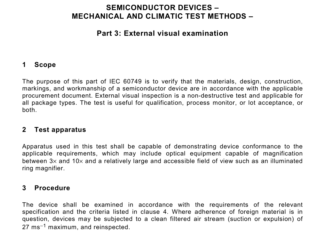
The purpose of this part of IEC 60749 is to verify that the materials, design, construction, markings, and workmanship of a semiconductor device are in accordance with the applicable procurement document. External visual inspection is a non-destructive test and applicable for all package types. The test is useful for qualification, process monitor, or lot acceptance, or both.
2 Test apparatus
Apparatus used in this test shall be capable of demonstrating device conformance to the applicable requirements, which may include optical equipment capable of magnification between 3× and 10× and a relatively large and accessible field of view such as an illuminated ring magnifier.
3 Procedure
The device shall be examined in accordance with the requirements of the relevant specification and the criteria listed in clause 4. Where adherence of foreign material is in question, devices may be subjected to a clean filtered air stream (suction or expulsion) of 27 ms −1 maximum, and reinspected.
4 Failure criteria
Devices shall be considered a failure if they exhibit any of the following: 4.1 Device design, terminal identification, markings (content, placement, and legibility), materials, construction, and workmanship, are not in accordance with the applicable procurement document. 4.2 Visible evidence of corrosion, contamination or breakage (grossly bent or broken terminals, cracked seals – except for glass meniscus), defective (peeling, flaking, or blistering) or damaged plating or exposed base metal. (Discoloration of the finish shall not be cause for failure unless there is evidence of flaking, pitting or corrosion.) 4.3 Terminals that are not intact and aligned in their normal location, free of sharp or unspecified terminal bends, and (for ribbon terminals) free of twist outside the normal terminal plane. 4.4 Terminals that are not free of foreign material such as paint or other adherent deposits. 4.5 Evidence of any non-conformance with the detail drawing or applicable procurement document, absence of any required feature, or evidence of damage, corrosion or contamination that will interfere with the normal application of the device.4.6 Defects or damage resulting from manufacturing, handling, testing, or the following: a) Cracked or broken packages. Surface scratches shall not be cause for failure, except where they violate other criteria stated herein for marking, finish, etc. b) Any chip-out dimension that exceeds 1,5 mm in any direction on the surface and has a depth that exceeds 25 % of the thickness of the affected package element (i.e. cover, base or wall). c) Any chip-out that exposes either sealing glass (not previously exposed prior to the chip- out) or any terminal frame material that is not intended to be exposed by design.
5 Summary
The following details shall be specified in the relevant specification: a) Requirements for markings and the terminal identification (see 4.1). b) Detailed requirements for materials, design, construction, and workmanship (see 4.1). c) Sample size.
